


Kalyan Koley
M.Tech. (National Institute of Technology, Silchar), PhD (Jadavpur University, Kolkata)
Date of Joining:
31st August, 2021
-
Department of Electronics and Communication Engineering, Birla Institute of Technology, Mesra, Ranchi, Jharkhand 835215
-
NA|NA
-
kalyan.koley@bitmesra.ac.in

Research Areas
- Modelling and simulations of emerging MOSFET
- CMOS circuit design for low power application
- Analog and Digital VLSI circuit design
- Compact modeling of CMOS devices

Work Experience
- Teaching: 9.6 Years
- Research: 1 Years




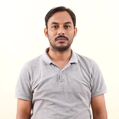 Kalyan
"
width="406"
height="371"
loading="lazy"
>
Academic Profile

Award and Honours

Project
Leadership & Institutional Service
Teaching & Mentorship
Award and Honours
INSA Visiting Scientist, Department of Electrical Engineering, Indian Institute of Technology, Kanpur, India (2026-2027)
Vice-Chairperson, IEEE Solid-State Circuits Society, Kolkata Section, India (2023-2025)
Vice-Chairperson, IEEE Solid-State Circuits Society, Kolkata Section, India (2021-2023)
Current Sponsored Projects
- Funding Agency: Department of Science and Technology, Government of India
- Project Cost: Rs. 35,00,000/- (Thirty Five Lakhs)
- Name of the Project: RF, Noise, and Harmonic Distortion Analysis of Structurally Modified Germanium on Insulator MOSFETS
- Duration: 5 years (February 2017 – January 2022)
Intellectual Property Rights (IPR)
-
A SYSTEM AND METHOD FOR ANALYSING RADIATION EFFECT ON GATE-ALL-AROUND TUNNEL TRANSISTOR
- Date: